The growing complexity of semiconductors brings a wider range of potential defects. Global random defects can only be reduced by long-term process improvement programs. Local defects are a result of controllable issues like equipment anomalies and inappropriate processing parameters.
Inspection systems evaluate patterned wafers for a wide variety of systematic and random defects that impact yield. Unlike a digital camera, which captures images one after another, these systems capture and evaluate entire wafers in a single pass.
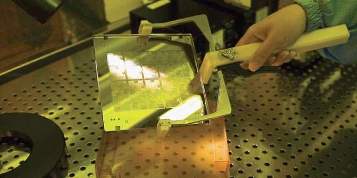
Manual
Die Prep Services Inspection is a critical part of the process of identifying defects in semiconductor wafers, which are thin slices of silicon used to create integrated circuits (ICs). Because ICs power most of today’s electronic devices, it’s important to find any defects as quickly and accurately as possible.
Bare wafers are typically tested at the manufacturer and again upon receipt at the fab to locate, map, and differentiate pre-existing defects from those created during the IC manufacturing process. Identifying these defects is essential for ensuring the highest quality chips possible.
Using the V2000 Bright Light, a dual-cassette macro defect inspection system, we can help you discover and classify all types of defects on your bare wafers or patterned wafers. It combines incredible macro defect inspection throughput with state-of-the-art software and analytics in an easy to use, versatile platform that’s designed to meet your needs. It’s a perfect solution for qualifying new materials and analyzing masks, reticles and wafers during the development stage.
Semi-Automated
Wafer inspection, the science of finding defects on a wafer, is becoming more challenging and costly at each new node due to process shrinks, design complexities, and new materials. Detecting micro defects with optical inspection tools is a daunting task and requires complex algorithms and specialized cameras.
EagleView automated macro defect semiconductor wafer inspection system delivers industry leading throughput, defect detection accuracy, and wafer classification for chip manufacturing. It eliminates many of the problems associated with manual and micro defect inspection by combining state-of-the-art robotics, imaging, and Microtronic ProcessGuard software to provide an unparalleled solution for 50 mm and 300 mm wafers.
Classification networks are an advanced image processing algorithm that uses neural network models to identify defects on a wafer surface. These algorithms can be used for a wide variety of applications including defect detection and wafer surface metrology. Classification networks are able to detect localized defects which can indicate equipment anomalies and inappropriate process parameters.
Fully-Automated
Fully-automated systems are fast, convenient, and efficient at high volumes. They are used to check every wafer in a batch and support production flow. These systems are more expensive than semi-automated and manual inspection systems.
In order to view critical backside defects (such as peeling and chipping) that can lead to catastrophic failure, a standard inspection system requires the wafer to be flipped during inspection. This can reduce a system’s throughput by half, cause die loss from the inverted tape and alignment issues with front to back side wafer map correlation.
Non-patterned wafer inspection (NSWI) systems measure the wafer surface using capacitance-based probes to evaluate a thousand points per minute. Unlike pattern-based inspection systems that use image comparison, NSWI uses coordinates to determine the area being inspected on the wafer. This allows for a more focused measurement and can exclude or include a wafer’s edges or center. NSWI is also useful for equipment condition checks by using dummy bare wafers to monitor equipment cleanliness.
Customized
Wafer inspection systems use a combination of bright-field or dark-field illumination for detecting defects. They work by comparing the image of a test die with the image of an adjacent die or “golden” die known to be defect free. Digital processing subtracts the two images, revealing any defects in the subtracted image. This allows a map of defect locations to be generated on the patterned wafer.
Wafer Dicing Services require precise and accurate motion control of both the wafer stage and optical components in the system. Our HybrYX hybrid air bearing XY stage provides extremely low velocity ripple and dynamic following error allowing wafer inspection systems to achieve high scanning velocities.
The Surfscan SP7XP unpatterned wafer inspection system detects surface quality defects that can impact the performance and reliability of leading-edge semiconductor devices. It helps IC, OEM and materials manufacturers qualify tools, processes and materials for EUV lithography as well as perform bare wafer outgoing and incoming quality control and wafer dispositioning.